Vitrek Highlights Growing Importance of Wafer Stress Characterization for Advanced Semiconductor Manufacturing
MTI Instruments Proforma™ non-contact wafer metrology systems help manufacturers optimize thin-film processes, improve process control, and increase production yield.
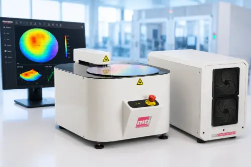
Lockport, IL — July 28, 2026— Vitrek, a leading manufacturer of precision test and measurement equipment, highlighted the growing importance of wafer stress measurement in semiconductor manufacturing as advanced packaging, heterogeneous integration, silicon carbide (SiC), gallium nitride (GaN), MEMS, and photonics applications continue to drive demand for tighter process control, improved manufacturing consistency, and higher device reliability.
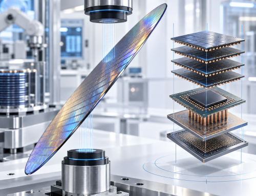
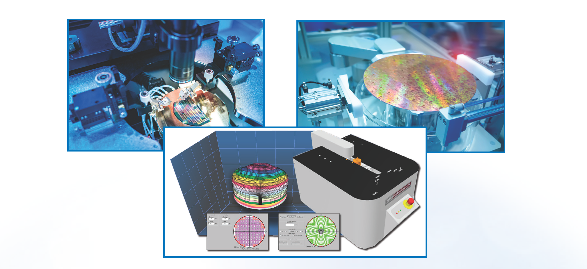
As semiconductor manufacturing processes become increasingly complex, engineers are placing greater emphasis on monitoring wafer stress to optimize thin-film deposition, validate process changes, detect equipment drift, and improve production yield. Full-wafer stress characterization provides valuable insight into process stability, enabling manufacturers to identify subtle variations before they impact downstream operations.
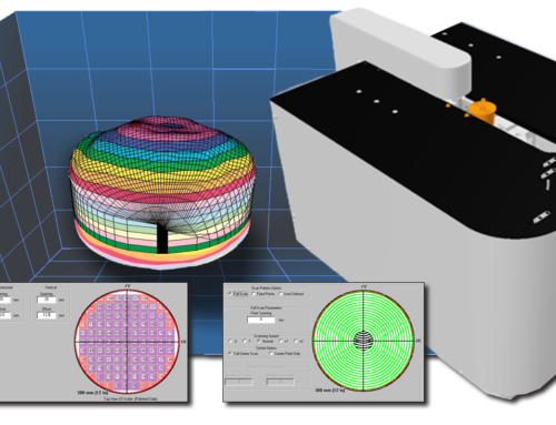
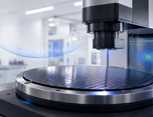
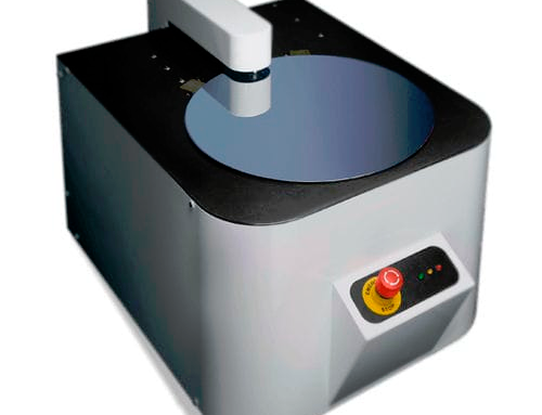
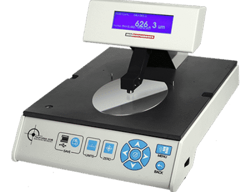
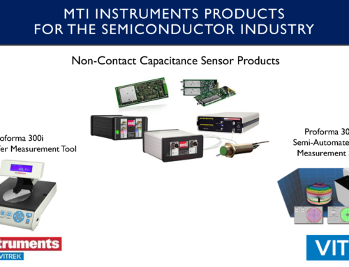
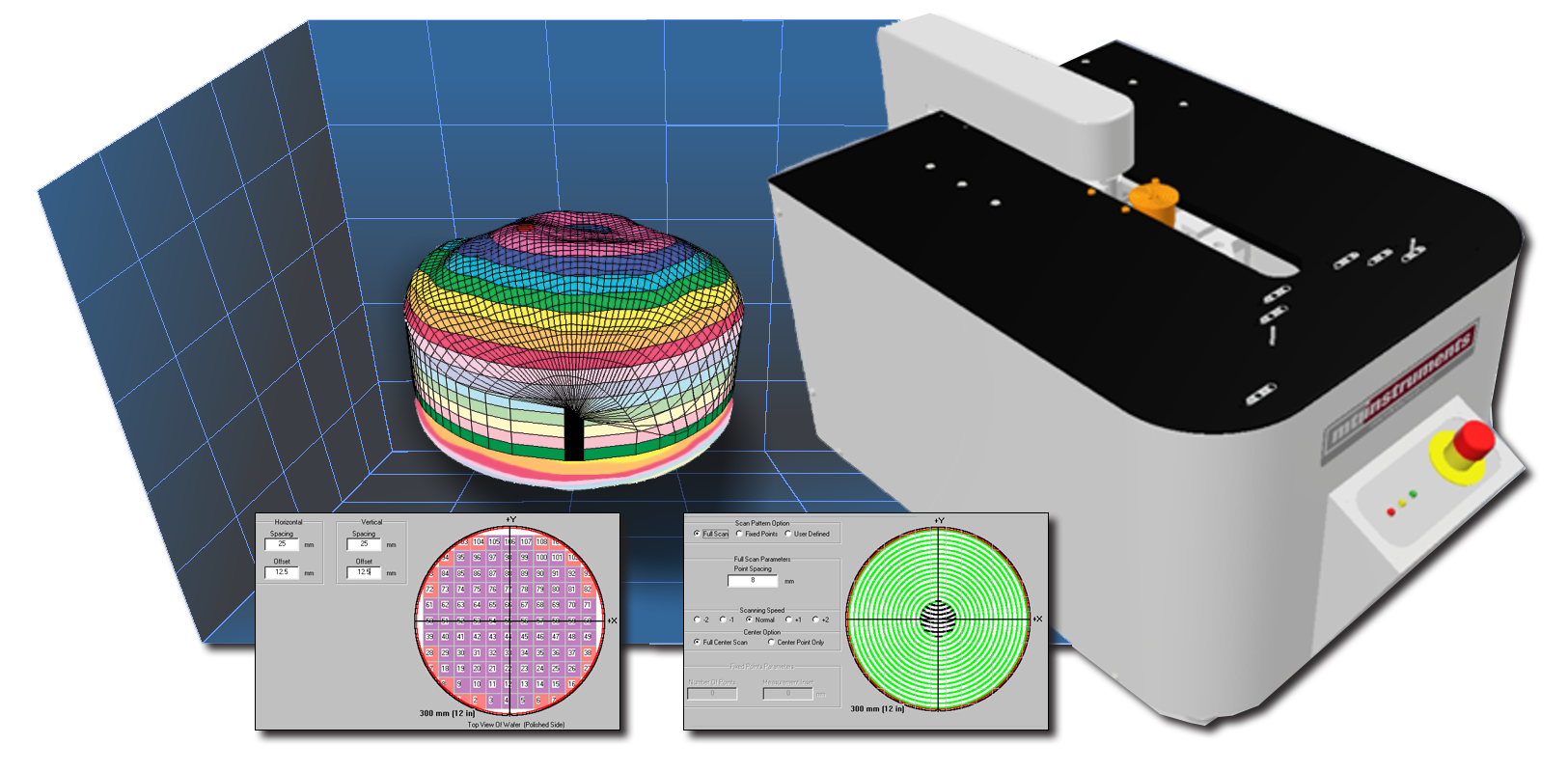
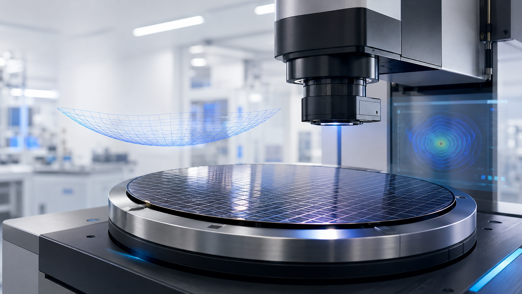
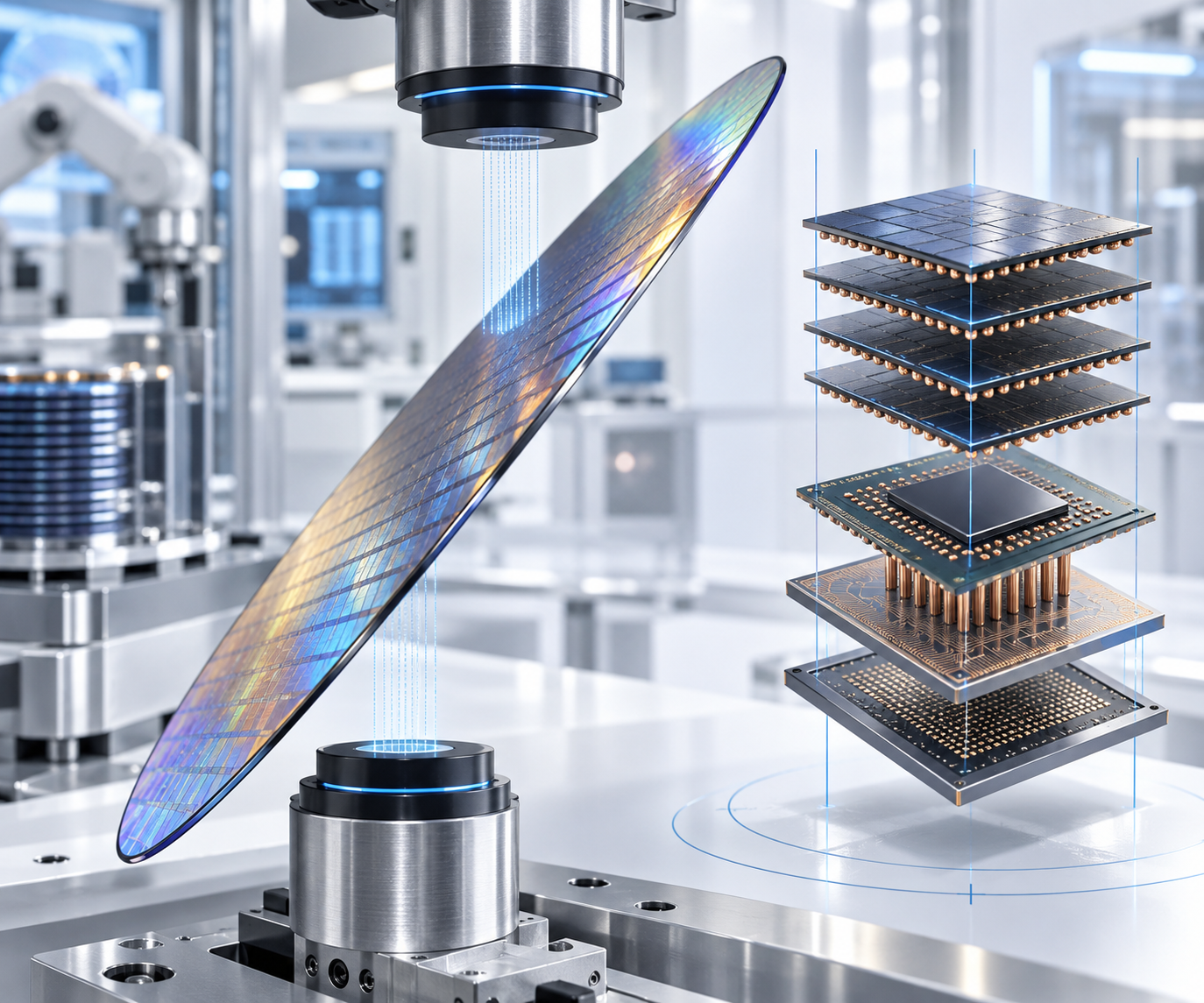
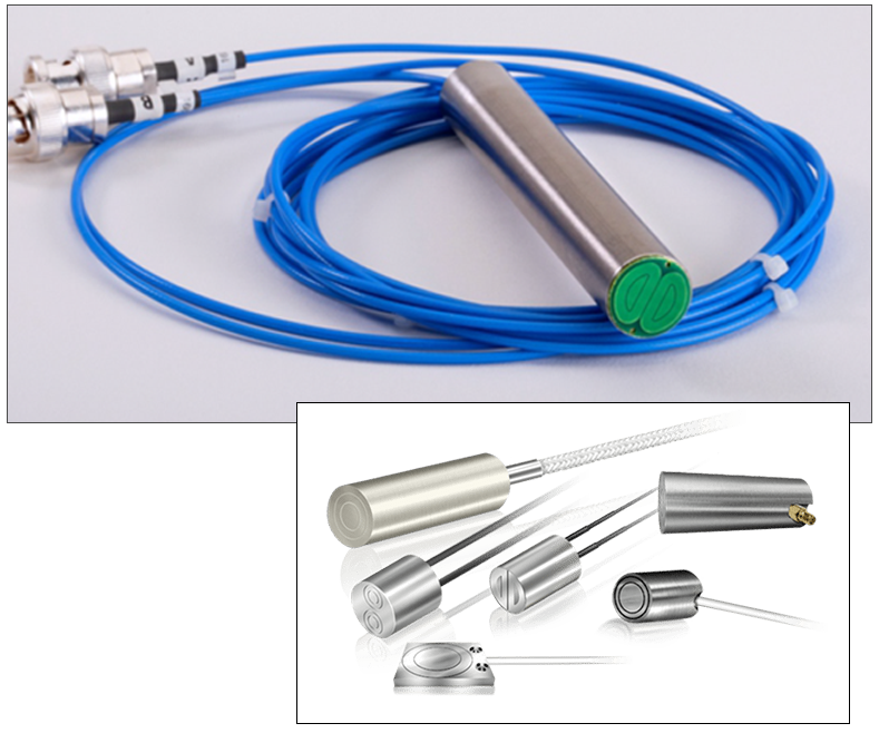
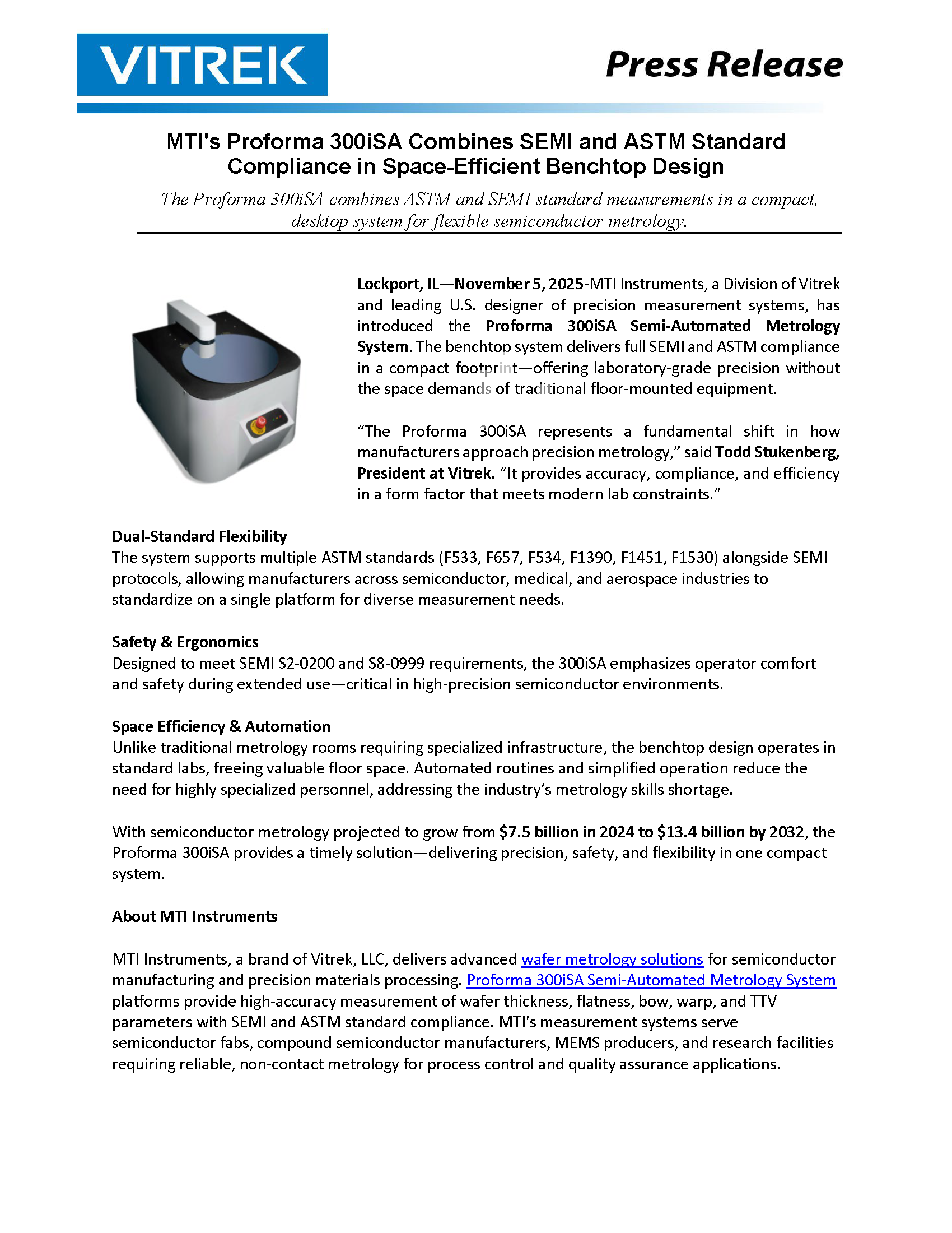
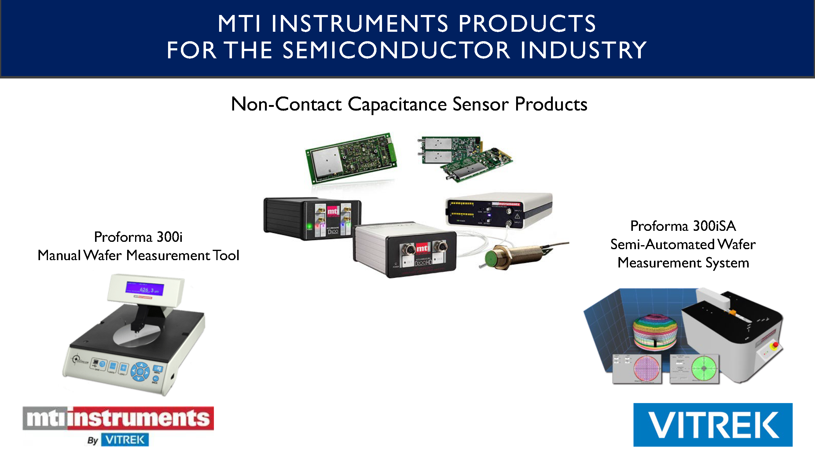
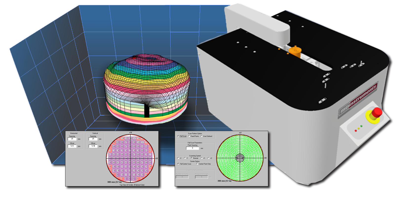
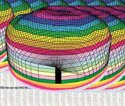
Vitrek’s Proforma™ family of non-contact wafer metrology systems provides high-precision measurement of wafer stress, bow, warp, curvature, thickness, and total thickness variation (TTV). By capturing comprehensive full-wafer measurement data, Proforma systems help engineers visualize stress distribution, evaluate process changes, and support statistical process control (SPC) initiatives throughout semiconductor manufacturing.
“Wafer stress has become much more than a laboratory measurement—it is now an important indicator of manufacturing performance,” said Ken Ameika, VP Global Sales at Vitrek. “Understanding how stress changes throughout fabrication enables engineers to optimize processes, improve repeatability, and support higher manufacturing yields.”
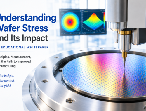
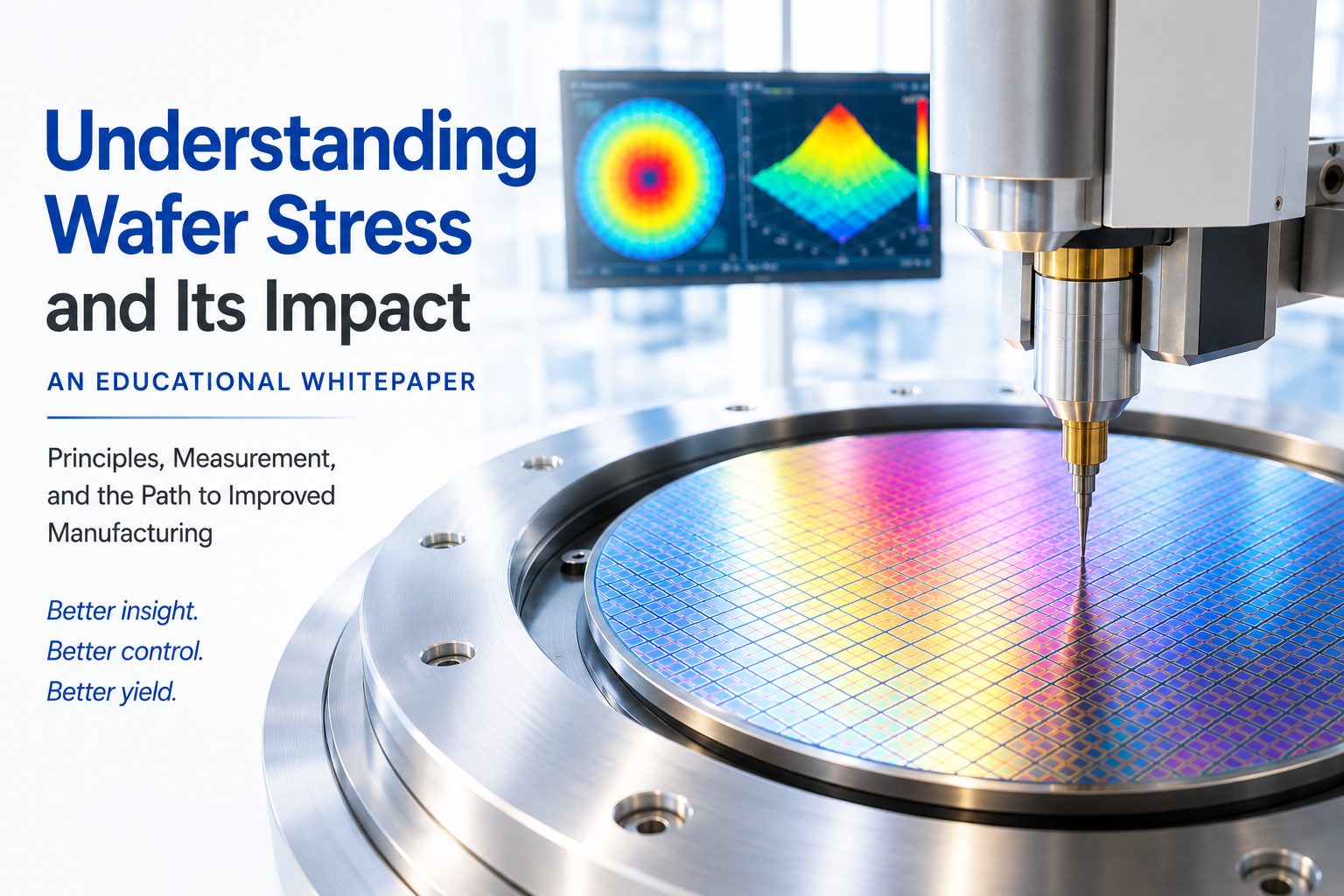
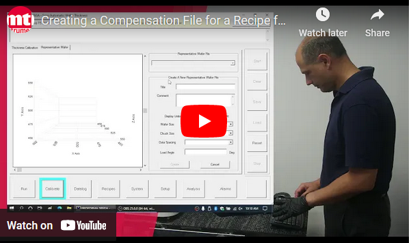
To help engineers better understand these challenges, Vitrek has published a new educational white paper, Understanding Wafer Stress, along with a companion application note, Characterizing Thin-Film Stress Using Full-Wafer Non-Contact Metrology. Together, these resources explore the principles of wafer stress and demonstrate how comprehensive non-contact wafer metrology supports modern semiconductor process control.
About Vitrek, LLC and the MTI Instruments Brand

Vitrek designs and manufactures precision test and measurement solutions for the semiconductor, aerospace, medical device, automotive, and electronics industries. The company’s MTI Instruments Proforma™ family of wafer metrology systems delivers accurate, repeatable non-contact measurements for research, process development, and production applications.