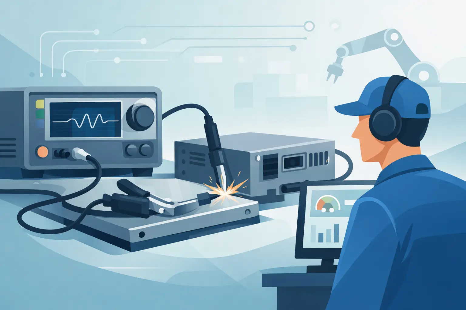
A defect that was inconsequential at 130 nm can be yield-limiting at advanced nodes, especially when it occurs in a critical layer or disrupts a three-dimensional device structure. That change is driving semiconductor inspection trends toward greater sensitivity, more complete wafer coverage, and measurement data that can be tied directly to process decisions. For fab engineers, yield teams, and equipment owners, the practical question is no longer whether to inspect more. It is how to obtain actionable information fast enough to control an increasingly complex process.
Semiconductor Inspection Trends: Inspection Is Becoming More Layer-Aware
The industry is moving beyond broad defect counts as a primary indicator of process health. A particle count alone does not reveal whether defects are electrically relevant, clustered around a specific tool, or concentrated on a layer with little process margin. Inspection strategies now increasingly account for layer context, defect type, location, and probable yield impact.
This shift matters because device architectures have changed the relationship between physical defects and electrical performance. FinFET, gate-all-around, advanced memory, image sensors, power semiconductors, and heterogeneous packages all introduce geometries where a small variation can have a disproportionate effect. A bridge, void, residue pattern, or edge defect may matter only under particular conditions, but those conditions must be identified before material moves too far downstream.
Layer-aware inspection does not mean applying the highest-sensitivity recipe to every wafer. That approach can overwhelm review capacity and generate nuisance signals. Instead, inspection plans are becoming risk-based. Critical layers receive tighter sampling or full-wafer inspection, while lower-risk layers may use optimized sampling plans. The right balance depends on device design, process maturity, known failure mechanisms, and the cost of delayed detection.
Higher Sensitivity Must Be Matched With Better Classification
As optical and electron-beam systems detect smaller features, fabs face a familiar operational problem: more detected events do not automatically produce more useful decisions. Detection sensitivity is necessary, but classification determines whether the data supports action.
A modern inspection flow needs to distinguish meaningful defects from process variation, patterned-background artifacts, benign particles, and repeating signatures that point to a common source. This requires correlation among inspection images, defect review, process-tool data, electrical test, and yield analysis. Machine learning can improve classification speed and consistency, particularly where large image sets contain recurring defect signatures. It does not remove the need for engineering judgment.
Classification models are only as reliable as the labeled data, process coverage, and validation methods behind them. A model trained on one product family or process revision may perform poorly after a material change, a new patterning sequence, or a tool chamber modification. Engineering teams should treat model monitoring, retraining, and false-call analysis as controlled parts of the inspection program rather than as one-time implementation work.
The most useful outcome is not simply an automated defect label. It is a prioritized queue that directs scarce review and failure-analysis resources toward defects most likely to affect yield, reliability, or customer quality.
Metrology and Inspection Are Converging
The boundary between inspection and metrology is becoming less distinct. Inspection identifies anomalies and excursions. Metrology quantifies dimensions, film properties, overlay, topography, and other process characteristics. In practice, both are required to explain why a process has shifted and whether the shift is within functional limits.
For example, a wafer may have no obvious random-defect excursion while still exhibiting a systematic dimensional trend that reduces process margin. Conversely, a metrology result can remain within specification while localized defects create yield loss. Combining these data sets gives engineers a more complete view of process behavior.
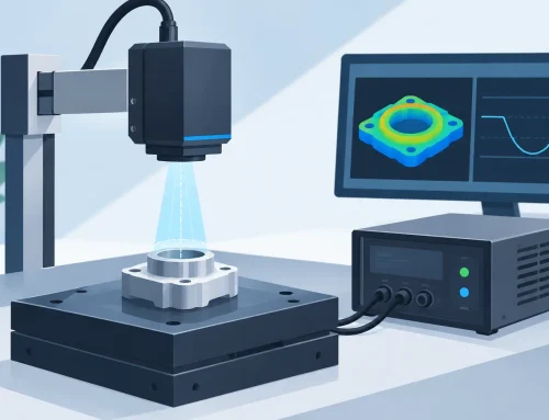
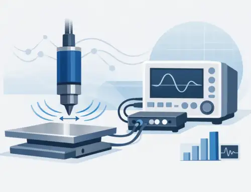
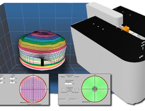
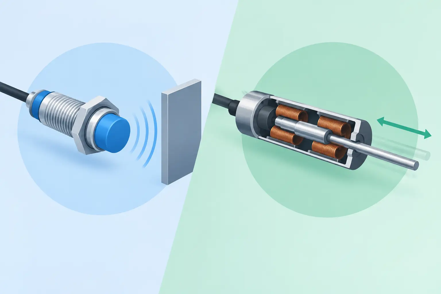
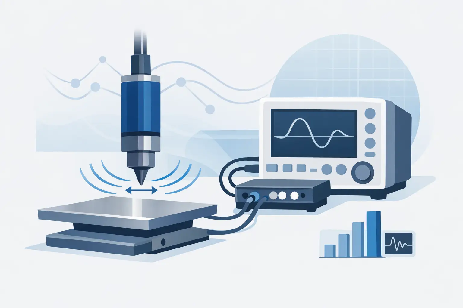
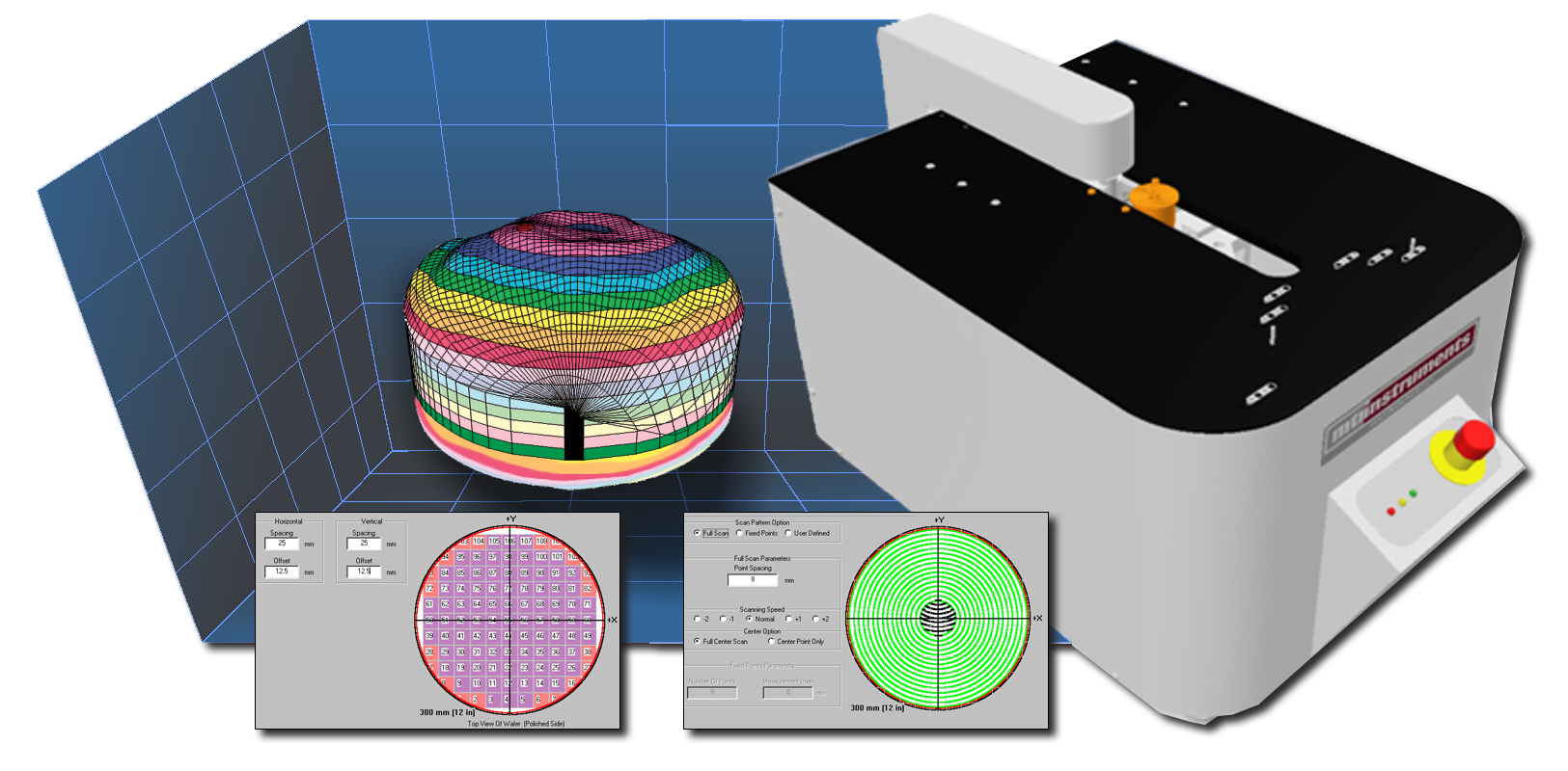
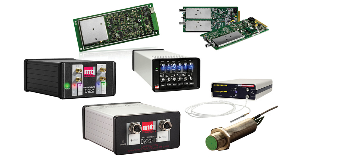
This convergence is particularly relevant for advanced packaging and compound semiconductor manufacturing. Wafer bow, surface topography, bump geometry, die placement, thin-film variation, and substrate characteristics can influence both assembly performance and long-term reliability. Non-contact measurement systems are valuable where fragile surfaces, small features, or tight repeatability requirements make contact methods unsuitable.
The measurement challenge is not limited to tool capability. Data must be traceable across lots, products, recipes, operators, and calibration events. Without that context, it becomes difficult to separate actual process drift from measurement-system variation.
Measurement System Performance Remains Foundational
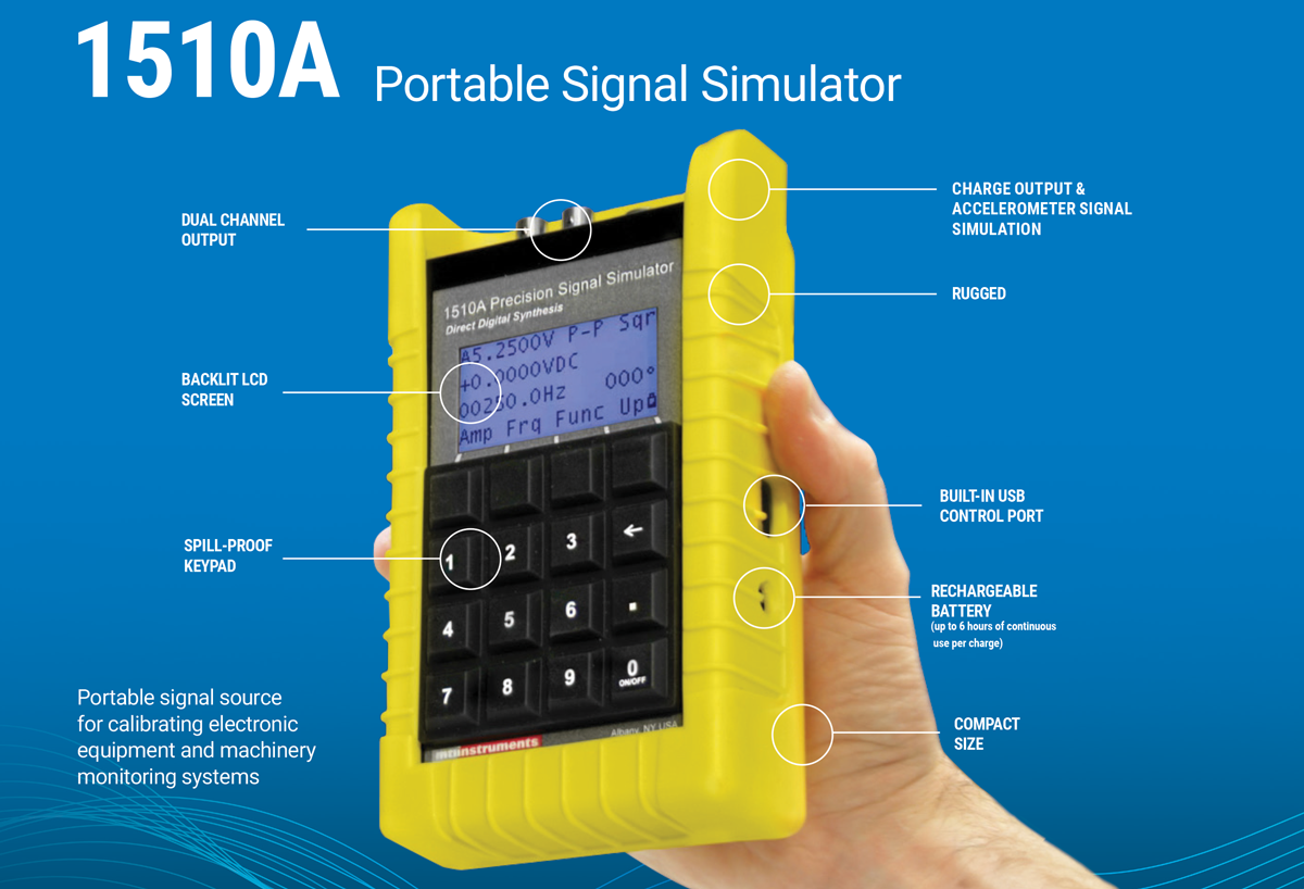
Higher-resolution inspection cannot compensate for an unstable measurement system. Repeatability, reproducibility, calibration traceability, environmental control, and recipe governance remain basic requirements. They become more demanding as process tolerances narrow.
Engineering teams should evaluate the full uncertainty chain, including sensor performance, fixturing, wafer handling, vibration, thermal effects, software calculations, and operator interaction. A measurement result can look precise while still being unsuitable for process control if these contributors are not understood.
For critical applications, the measurement system should support documented calibration practices and data integrity requirements that align with the organization’s quality system. This is especially relevant when inspection and metrology records support customer qualification, regulated product manufacturing, or root-cause investigations.
Faster Feedback Is More Valuable Than More Data
One of the most consequential semiconductor inspection trends is the drive to shorten the loop between detection and corrective action. A defect found after multiple downstream process steps may identify a problem, but it may also represent lost wafers, delayed engineering work, and a larger containment effort. Earlier detection limits exposure.
This is leading fabs to integrate inspection results more closely with manufacturing execution systems, statistical process control, equipment histories, and automated disposition workflows. The objective is not fully autonomous manufacturing in every case. It is to reduce the time spent moving data between disconnected systems and to present the right evidence when an engineer needs to make a decision.
Effective feedback systems typically connect four elements:
- Inspection and metrology results with consistent wafer, lot, and process-step identifiers.
- Equipment-state data, maintenance history, and chamber or consumable changes.
- Review and classification results that identify likely defect mechanisms.
- Escalation rules that distinguish routine variation from events requiring immediate engineering attention.
The trade-off is integration complexity. Data pipelines, interfaces, access controls, and recipe management require disciplined ownership. A poorly governed automated alert system can create alarm fatigue or trigger unnecessary holds. Teams should begin with a defined set of high-value use cases, such as identifying a recurring defect signature after preventive maintenance or correlating edge exclusions with a specific wafer-handling condition.
Advanced Packaging Is Expanding the Inspection Scope
Inspection requirements no longer end at front-end wafer processing. Chiplets, 2.5D and 3D integration, hybrid bonding, fan-out wafer-level packaging, and high-density interconnects shift more quality risk into packaging and assembly steps.
These processes require inspection approaches that can address surface contamination, alignment, bond quality, bump coplanarity, substrate warpage, placement accuracy, and buried interconnect features. The inspection method must fit the defect mechanism. Optical techniques offer speed and broad coverage for many surface conditions. X-ray, acoustic, electron-beam, and specialized non-contact metrology may be necessary when defects are buried, dimensions are extremely small, or material contrast is limited.
No single modality is optimal across the entire flow. Equipment selection should be tied to the failure modes that matter most, the throughput required, and the point at which information can still change the outcome. A highly capable system that delivers results too late for corrective action has limited production value.
Data Architecture Is Now an Inspection Requirement
Inspection data volumes continue to grow, but storage capacity alone is not the issue. The central requirement is usable data architecture. Engineers need to compare results across tools, products, shifts, and process revisions without losing the context that makes those comparisons valid.
Standardized naming, recipe version control, synchronized timestamps, retained raw data where appropriate, and clear access permissions all contribute to trustworthy analysis. So does the ability to export data into existing yield-management, statistical analysis, and factory automation environments. Proprietary data silos can slow root-cause work, particularly when a defect spans multiple equipment types or manufacturing stages.
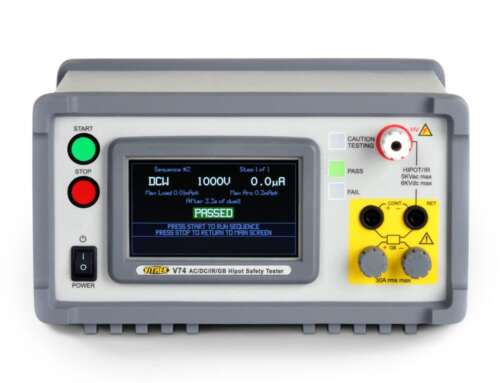
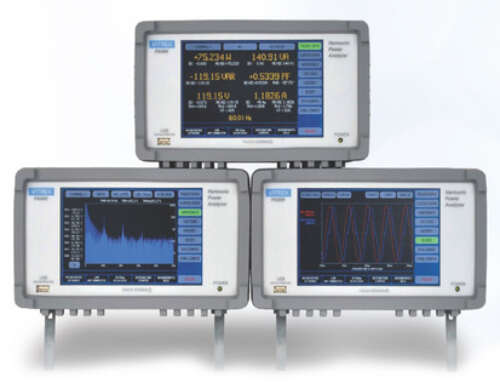
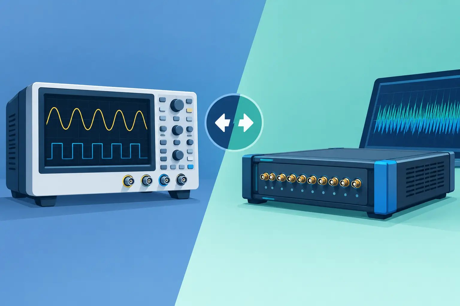
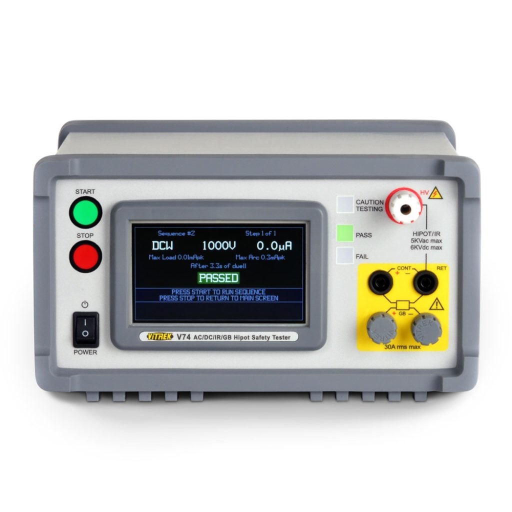
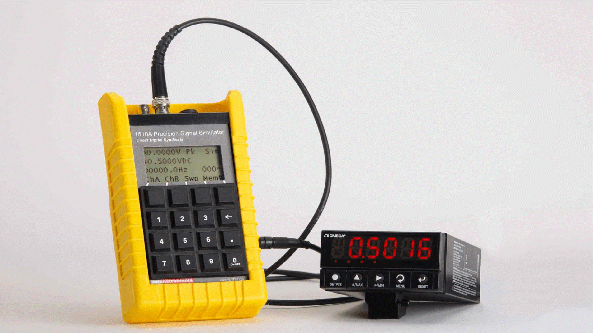
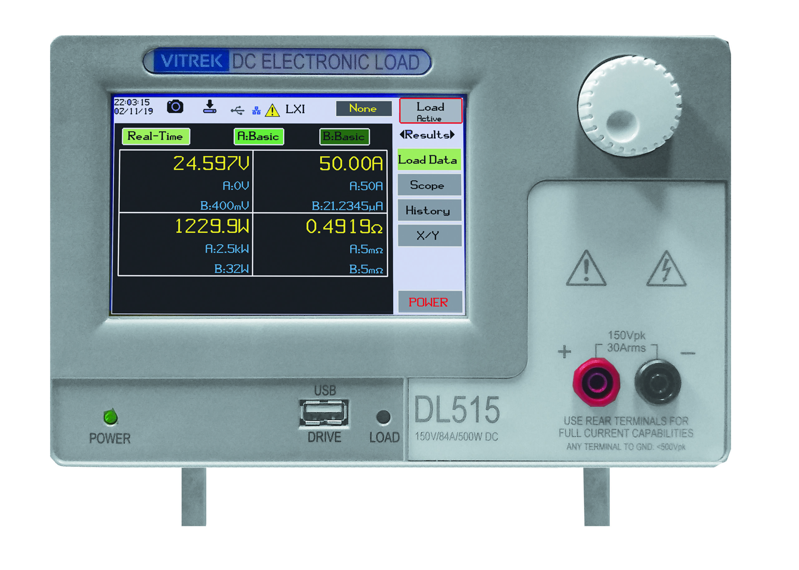
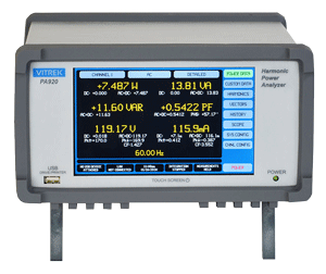
For organizations modernizing older test infrastructure, interoperability should be evaluated as carefully as measurement performance. Instrument software, SDK support, data formats, and long-term serviceability influence whether a measurement platform remains useful as factory systems evolve. Vitrek’s measurement and metrology capabilities reflect this broader need for accurate, repeatable data that can support engineering decisions beyond a single test station.
The Practical Direction for Inspection Programs
The strongest inspection programs are not necessarily the ones with the most data or the highest nominal resolution. They are the programs that connect sensitivity to yield relevance, measurement integrity to process control, and detection speed to a clear response path.
As device structures, materials, and packaging methods continue to change, inspection strategies should be reviewed against actual failure mechanisms rather than inherited from prior technology generations. A disciplined assessment of defect risk, metrology uncertainty, review capacity, and data flow can reveal where additional capability will have the greatest effect. The objective is straightforward: detect the conditions that matter early enough, accurately enough, and consistently enough to protect yield.